
The demand for advanced material characterization has increased significantly across industries such as nanotechnology, semiconductors, metallurgy, pharmaceuticals, electronics, and energy. Researchers and manufacturers require detailed insights into material structures at the atomic scale to improve product quality, enhance performance, and drive innovation. This is where HRTEM Testing Labs in India play a crucial role.
High-Resolution Transmission Electron Microscopy (HRTEM) is one of the most sophisticated analytical techniques available today. It allows scientists to visualize individual atomic planes, crystal defects, nanoparticles, grain boundaries, and interfaces with exceptional clarity. However, achieving reliable atomic-level imaging requires more than just advanced equipment. It depends on expert sample preparation, instrument calibration, experienced analysts, and standardized testing procedures.
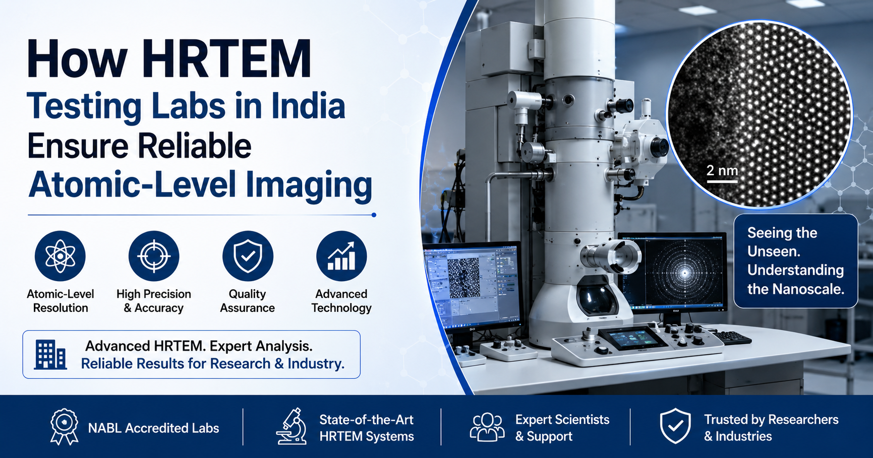
What is HRTEM?
High-Resolution Transmission Electron Microscopy (HRTEM) is an advanced microscopy technique that uses a high-energy electron beam to image materials at atomic or near-atomic resolution.
Unlike conventional optical microscopes, HRTEM can reveal:
- Atomic lattice structures
- Crystal orientation
- Grain boundaries
- Crystal defects
- Dislocations
- Nanoparticles
- Interfaces between different materials
- Thin-film structures
Modern HRTEM instruments can achieve resolutions below one nanometer, making them indispensable for cutting-edge research and industrial quality analysis.
Why Atomic-Level Imaging Matters
Atomic-level imaging provides valuable insights that are impossible to obtain using conventional microscopy techniques.
It helps researchers:
- Understand material behavior
- Improve product reliability
- Develop advanced nanomaterials
- Analyze manufacturing defects
- Optimize semiconductor devices
- Study catalyst performance
- Investigate battery materials
- Validate crystal structures
Reliable imaging ensures that scientific conclusions and industrial decisions are based on accurate structural information.
How HRTEM Testing Labs in India Ensure Reliable Results
1. Advanced High-Resolution Electron Microscopes
Leading HRTEM Testing Labs in India invest in state-of-the-art transmission electron microscopes equipped with:
- High-brightness electron sources
- Field emission guns (FEG)
- Aberration correction systems
- High-resolution CCD and CMOS detectors
- Digital imaging software
- Automated alignment systems
These technologies significantly improve image clarity while minimizing distortions.
2. Expert Sample Preparation
Sample preparation is often considered the most critical step in HRTEM analysis.
Even the most advanced microscope cannot produce accurate results if the sample is poorly prepared.
Professional laboratories use specialized preparation techniques such as:
- Focused Ion Beam (FIB) milling
- Ion polishing
- Ultramicrotomy
- Mechanical thinning
- Precision polishing
- Cryogenic preparation for sensitive materials
These methods produce electron-transparent specimens without introducing structural damage.
3. Precise Instrument Calibration
Reliable atomic imaging requires continuous calibration of the microscope.
Testing laboratories routinely perform:
- Beam alignment
- Lens calibration
- Magnification verification
- Resolution testing
- Astigmatism correction
- Drift compensation
Regular calibration ensures consistent imaging performance throughout every analysis.
4. Controlled Laboratory Environment
Environmental conditions directly affect image quality.
Professional HRTEM laboratories maintain:
- Temperature-controlled rooms
- Low vibration environments
- Electromagnetic shielding
- Dust-free facilities
- Stable electrical power supply
These conditions reduce noise and improve image stability during high-magnification imaging.
5. Highly Skilled Microscopists
Operating an HRTEM instrument requires years of experience.
Experienced scientists understand:
- Electron beam interactions
- Material behavior
- Imaging artifacts
- Diffraction patterns
- Crystallographic analysis
- Data interpretation
Their expertise helps distinguish genuine material features from imaging artifacts.
6. Multiple Imaging Techniques
Reliable analysis rarely depends on a single image.
Most HRTEM Testing Labs in India combine multiple characterization techniques, including:
- Bright Field TEM
- Dark Field TEM
- High-Resolution TEM
- Selected Area Electron Diffraction (SAED)
- Scanning TEM (STEM)
- Energy Dispersive X-ray Spectroscopy (EDS)
- Electron Energy Loss Spectroscopy (EELS)
Combining these methods provides a comprehensive understanding of material composition and structure.
7. Advanced Digital Image Processing
Modern HRTEM systems include advanced software for:
- Image enhancement
- Noise reduction
- Lattice spacing measurement
- Particle size analysis
- Defect mapping
- Crystal orientation analysis
- Fast Fourier Transform (FFT)
Digital analysis improves accuracy while preserving original structural information.
8. Standardized Testing Protocols
Accredited laboratories follow standardized operating procedures to ensure consistent testing quality.
These include:
- Sample documentation
- Instrument validation
- Calibration records
- Data verification
- Image quality assessment
- Repeatability checks
- Detailed reporting
Standardization minimizes errors and enhances result reliability.
Industries That Depend on HRTEM Testing
HRTEM testing supports numerous research and industrial sectors.
Semiconductor Industry
- Defect analysis
- Thin-film characterization
- Failure analysis
- Process optimization
Nanotechnology
- Nanoparticle imaging
- Nanocomposite evaluation
- Quantum material research
Metallurgy
- Grain boundary analysis
- Phase identification
- Alloy characterization
Pharmaceuticals
- Drug particle characterization
- Nanomedicine research
- Crystal morphology analysis
Energy Storage
- Battery electrode analysis
- Fuel cell research
- Supercapacitor development
Aerospace
- Composite material evaluation
- High-strength alloy analysis
- Failure investigations
Benefits of Choosing Professional HRTEM Testing Labs in India
Working with an experienced HRTEM laboratory offers several advantages:
- Accurate atomic-level imaging
- Reliable crystallographic analysis
- High-resolution structural characterization
- Expert interpretation of results
- Faster turnaround time
- Comprehensive technical reports
- Advanced analytical capabilities
- Cost-effective testing solutions
Factors to Consider When Selecting an HRTEM Testing Laboratory
Choosing the right laboratory is essential for obtaining dependable results.
Consider the following factors:
- Availability of modern HRTEM equipment
- Experienced microscopy specialists
- Comprehensive sample preparation facilities
- Accreditation and quality standards
- Advanced analytical capabilities
- Turnaround time
- Technical consultation support
- Clear and detailed reporting
A well-equipped laboratory ensures both accuracy and reproducibility.
Future of HRTEM Testing in India
The future of HRTEM testing is closely linked to advancements in materials science and nanotechnology. Emerging trends include:
- AI-assisted image analysis
- Automated defect detection
- Cryogenic electron microscopy
- In-situ HRTEM experimentation
- 3D electron tomography
- Machine learning for crystal analysis
- Faster digital image processing
- Integration with multi-modal characterization techniques
As research and manufacturing become increasingly sophisticated, HRTEM testing laboratories will continue to play a pivotal role in enabling innovation.
Conclusion
High-Resolution Transmission Electron Microscopy has transformed the way researchers study materials at the atomic scale. From semiconductor devices and nanomaterials to advanced alloys and pharmaceuticals, HRTEM provides unparalleled insights into material structure and performance.
HRTEM Testing Labs in India ensure reliable atomic-level imaging through advanced instrumentation, meticulous sample preparation, rigorous calibration, skilled scientists, and standardized testing protocols. Their expertise enables industries and research organizations to make informed decisions, improve product quality, and accelerate scientific discovery.
As technology continues to evolve, HRTEM testing will remain an essential tool for solving complex material challenges and driving innovation across diverse sectors.
Frequently Asked Questions
1. What is HRTEM used for?
HRTEM is used to visualize materials at atomic resolution, analyze crystal structures, identify defects, and characterize nanomaterials.
2. Which industries benefit from HRTEM testing?
Industries such as semiconductors, nanotechnology, metallurgy, pharmaceuticals, aerospace, electronics, and energy storage commonly use HRTEM analysis.
3. Why is sample preparation important in HRTEM?
Proper sample preparation ensures electron transparency, minimizes structural damage, and improves imaging accuracy.
4. Can HRTEM identify crystal defects?
Yes. HRTEM can detect dislocations, grain boundaries, vacancies, stacking faults, and other crystal defects at the atomic scale.
5. How do HRTEM Testing Labs in India ensure reliable results?
They combine advanced microscopy systems, expert sample preparation, routine calibration, controlled laboratory environments, standardized procedures, and experienced analysts to deliver accurate and reproducible atomic-level imaging.
The demand for advanced material characterization has increased significantly across industries such as nanotechnology, semiconductors, metallurgy, pharmaceuticals, electronics, and energy. Researchers and manufacturers require detailed insights into material structures at the atomic scale to improve product quality, enhance performance, and drive innovation. This is where HRTEM Testing Labs in India play a crucial role.
High-Resolution Transmission Electron Microscopy (HRTEM) is one of the most sophisticated analytical techniques available today. It allows scientists to visualize individual atomic planes, crystal defects, nanoparticles, grain boundaries, and interfaces with exceptional clarity. However, achieving reliable atomic-level imaging requires more than just advanced equipment. It depends on expert sample preparation, instrument calibration, experienced analysts, and standardized testing procedures.
What is HRTEM?
High-Resolution Transmission Electron Microscopy (HRTEM) is an advanced microscopy technique that uses a high-energy electron beam to image materials at atomic or near-atomic resolution.
Unlike conventional optical microscopes, HRTEM can reveal:
- Atomic lattice structures
- Crystal orientation
- Grain boundaries
- Crystal defects
- Dislocations
- Nanoparticles
- Interfaces between different materials
- Thin-film structures
Modern HRTEM instruments can achieve resolutions below one nanometer, making them indispensable for cutting-edge research and industrial quality analysis.
Why Atomic-Level Imaging Matters
Atomic-level imaging provides valuable insights that are impossible to obtain using conventional microscopy techniques.
It helps researchers:
- Understand material behavior
- Improve product reliability
- Develop advanced nanomaterials
- Analyze manufacturing defects
- Optimize semiconductor devices
- Study catalyst performance
- Investigate battery materials
- Validate crystal structures
Reliable imaging ensures that scientific conclusions and industrial decisions are based on accurate structural information.
How HRTEM Testing Labs in India Ensure Reliable Results
1. Advanced High-Resolution Electron Microscopes
Leading HRTEM Testing Labs in India invest in state-of-the-art transmission electron microscopes equipped with:
- High-brightness electron sources
- Field emission guns (FEG)
- Aberration correction systems
- High-resolution CCD and CMOS detectors
- Digital imaging software
- Automated alignment systems
These technologies significantly improve image clarity while minimizing distortions.
2. Expert Sample Preparation
Sample preparation is often considered the most critical step in HRTEM analysis.
Even the most advanced microscope cannot produce accurate results if the sample is poorly prepared.
Professional laboratories use specialized preparation techniques such as:
- Focused Ion Beam (FIB) milling
- Ion polishing
- Ultramicrotomy
- Mechanical thinning
- Precision polishing
- Cryogenic preparation for sensitive materials
These methods produce electron-transparent specimens without introducing structural damage.
3. Precise Instrument Calibration
Reliable atomic imaging requires continuous calibration of the microscope.
Testing laboratories routinely perform:
- Beam alignment
- Lens calibration
- Magnification verification
- Resolution testing
- Astigmatism correction
- Drift compensation
Regular calibration ensures consistent imaging performance throughout every analysis.
4. Controlled Laboratory Environment
Environmental conditions directly affect image quality.
Professional HRTEM laboratories maintain:
- Temperature-controlled rooms
- Low vibration environments
- Electromagnetic shielding
- Dust-free facilities
- Stable electrical power supply
These conditions reduce noise and improve image stability during high-magnification imaging.
5. Highly Skilled Microscopists
Operating an HRTEM instrument requires years of experience.
Experienced scientists understand:
- Electron beam interactions
- Material behavior
- Imaging artifacts
- Diffraction patterns
- Crystallographic analysis
- Data interpretation
Their expertise helps distinguish genuine material features from imaging artifacts.
6. Multiple Imaging Techniques
Reliable analysis rarely depends on a single image.
Most HRTEM Testing Labs in India combine multiple characterization techniques, including:
- Bright Field TEM
- Dark Field TEM
- High-Resolution TEM
- Selected Area Electron Diffraction (SAED)
- Scanning TEM (STEM)
- Energy Dispersive X-ray Spectroscopy (EDS)
- Electron Energy Loss Spectroscopy (EELS)
Combining these methods provides a comprehensive understanding of material composition and structure.
7. Advanced Digital Image Processing
Modern HRTEM systems include advanced software for:
- Image enhancement
- Noise reduction
- Lattice spacing measurement
- Particle size analysis
- Defect mapping
- Crystal orientation analysis
- Fast Fourier Transform (FFT)
Digital analysis improves accuracy while preserving original structural information.
8. Standardized Testing Protocols
Accredited laboratories follow standardized operating procedures to ensure consistent testing quality.
These include:
- Sample documentation
- Instrument validation
- Calibration records
- Data verification
- Image quality assessment
- Repeatability checks
- Detailed reporting
Standardization minimizes errors and enhances result reliability.
Industries That Depend on HRTEM Testing
HRTEM testing supports numerous research and industrial sectors.
Semiconductor Industry
- Defect analysis
- Thin-film characterization
- Failure analysis
- Process optimization
Nanotechnology
- Nanoparticle imaging
- Nanocomposite evaluation
- Quantum material research
Metallurgy
- Grain boundary analysis
- Phase identification
- Alloy characterization
Pharmaceuticals
- Drug particle characterization
- Nanomedicine research
- Crystal morphology analysis
Energy Storage
- Battery electrode analysis
- Fuel cell research
- Supercapacitor development
Aerospace
- Composite material evaluation
- High-strength alloy analysis
- Failure investigations
Benefits of Choosing Professional HRTEM Testing Labs in India
Working with an experienced HRTEM laboratory offers several advantages:
- Accurate atomic-level imaging
- Reliable crystallographic analysis
- High-resolution structural characterization
- Expert interpretation of results
- Faster turnaround time
- Comprehensive technical reports
- Advanced analytical capabilities
- Cost-effective testing solutions
Factors to Consider When Selecting an HRTEM Testing Laboratory
Choosing the right laboratory is essential for obtaining dependable results.
Consider the following factors:
- Availability of modern HRTEM equipment
- Experienced microscopy specialists
- Comprehensive sample preparation facilities
- Accreditation and quality standards
- Advanced analytical capabilities
- Turnaround time
- Technical consultation support
- Clear and detailed reporting
A well-equipped laboratory ensures both accuracy and reproducibility.
Future of HRTEM Testing in India
The future of HRTEM testing is closely linked to advancements in materials science and nanotechnology. Emerging trends include:
- AI-assisted image analysis
- Automated defect detection
- Cryogenic electron microscopy
- In-situ HRTEM experimentation
- 3D electron tomography
- Machine learning for crystal analysis
- Faster digital image processing
- Integration with multi-modal characterization techniques
As research and manufacturing become increasingly sophisticated, HRTEM testing laboratories will continue to play a pivotal role in enabling innovation.
Conclusion
High-Resolution Transmission Electron Microscopy has transformed the way researchers study materials at the atomic scale. From semiconductor devices and nanomaterials to advanced alloys and pharmaceuticals, HRTEM provides unparalleled insights into material structure and performance.
HRTEM Testing Labs in India ensure reliable atomic-level imaging through advanced instrumentation, meticulous sample preparation, rigorous calibration, skilled scientists, and standardized testing protocols. Their expertise enables industries and research organizations to make informed decisions, improve product quality, and accelerate scientific discovery.
As technology continues to evolve, HRTEM testing will remain an essential tool for solving complex material challenges and driving innovation across diverse sectors.
Frequently Asked Questions
1. What is HRTEM used for?
HRTEM is used to visualize materials at atomic resolution, analyze crystal structures, identify defects, and characterize nanomaterials.
2. Which industries benefit from HRTEM testing?
Industries such as semiconductors, nanotechnology, metallurgy, pharmaceuticals, aerospace, electronics, and energy storage commonly use HRTEM analysis.
3. Why is sample preparation important in HRTEM?
Proper sample preparation ensures electron transparency, minimizes structural damage, and improves imaging accuracy.
4. Can HRTEM identify crystal defects?
Yes. HRTEM can detect dislocations, grain boundaries, vacancies, stacking faults, and other crystal defects at the atomic scale.
5. How do HRTEM Testing Labs in India ensure reliable results?
They combine advanced microscopy systems, expert sample preparation, routine calibration, controlled laboratory environments, standardized procedures, and experienced analysts to deliver accurate and reproducible atomic-level imaging.